
Is glass substrate finished? What is a SiC interposer?
The End of the Glass Substrate Myth? Has the Winner in Semiconductor Packaging Already Been Decided?

NVIDIA’s massive performance gains don’t come for free.
They demand a sacrifice in the form of enormous power consumption and heat generation.
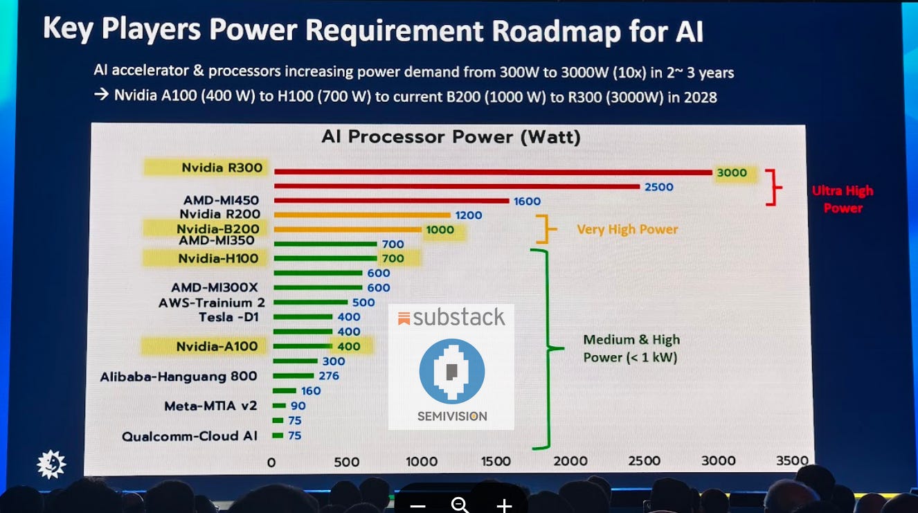
Take a look at the picture above.
Taiwan’s supply chain is speculating that Rubin Ultra’s power consumption could reach as high as 3,000 watts.
To put that in perspective, that’s about three times the power draw of the Blackwell B200, an enormous leap.
And it’s not just about higher electricity bills — with greater power consumption inevitably comes massive heat generation as well.
Because of this rising heat problem, what’s getting attention these days are substrates and interposers. The reason is simple: existing interposers and substrates can no longer withstand such levels of heat and power consumption.
It’s easy to dismiss substrates and interposers as low value-added industries, but in today’s AI era, they are in fact the invisible infrastructure that supports computing performance. The way you lay out the data pathways between chips, or between chips and memory, can determine the performance of the entire system.
This is especially true for high-bandwidth memory (HBM), the heart of AI accelerators. To solve the bottleneck in HBM, interposer and substrate technologies are receiving more attention than ever.
Why is resolving the HBM bottleneck so critical? Because no matter how fast a GPU is, if a memory bottleneck occurs, training and inference speeds plummet. That’s why the industry is betting heavily on packaging technologies that can maximize HBM’s performance.
The problem, however, is that interposers and substrates are now emerging as the weakest link. In environments where tens to hundreds of GB/s of data must flow, what’s needed is not just a connector material, but a high value-added solution with optimized electrical and thermal characteristics.
This is where a new competitive dynamic comes in. For years, the industry has viewed glass substrates as the next-generation answer. With their low dielectric constant, ability to handle large-area processing, and relatively low cost, they were expected to be a perfect fit for the expansion of HBM and HPC chips. In fact, global materials suppliers and substrate makers in Korea and Japan have been pouring large investments into mass production of glass substrates.
But recently, another contender has been rapidly gaining ground: the SiC (silicon carbide) interposer. Originally known as a power semiconductor material, SiC offers high thermal conductivity and strong mechanical stability, making it well-suited for packaging next-generation AI accelerators with extreme power consumption and heat output. Especially in environments that require both 3D-stacked HBM and ultra-high-speed I/O, SiC is increasingly being touted as more reliable than glass substrates.
This leads to a key question: if the adoption of SiC interposers accelerates, can glass substrates still hold their place as the star of next-generation packaging? Or will they be pushed aside from a “future technology” to merely an “alternative” before living up to expectations? This article aims to explore that very tension — the balance of power between SiC and glass substrates, and the ripple effects that will follow.
About glass substrates
There are two types of glass substrates.
One is the glass core substrate, and the other is the glass interposer, which replaces the currently used silicon interposer with glass.
![특징주] AI 확산에 반도체 유리 기판株 강세… 와이씨켐, 18% 상승](https://substackcdn.com/image/fetch/$s_!8KPI!,f_auto,q_auto:good,fl_progressive:steep/https%3A%2F%2Fsubstack-post-media.s3.amazonaws.com%2Fpublic%2Fimages%2F6db4b953-1ba3-47e2-92c9-c4d0adba2352_658x355.jpeg "특징주] AI 확산에 반도체 유리 기판株 강세… 와이씨켐, 18% 상승")
Currently, the field where players in the industry are relatively trying to enter more actively is the glass core substrate.
A glass core substrate means that the core material inside today’s substrates — which is plastic, specifically FR4 — holds the center.
What GCS aims to do is, as shown on the right, replace that central core with glass.
Then what advantages would it bring if we replace this with glass?
It is advantageous for large-area processing, meaning multiple semiconductors can be packaged at once.
It is also beneficial for miniaturization, as it allows the wiring width of the package substrate to be significantly reduced compared to today.

In fact, the reason glass substrates have received so much attention is none other than because Intel is leading the way.
For the past 50 years, Intel has been the emperor of semiconductors, and even though its dominance has been shaken in recent years, it still supplies an enormous volume of semiconductors worldwide when you look at shipment numbers.
So then, what exactly is a glass interposer?
A glass interposer is the medium that connects the chip and the substrate from the top side of the package substrate. In terms of TSMC’s 2.5D packaging technology, CoWoS (Chip-on-Wafer-on-Substrate), the ‘W’ corresponds to the glass interposer. Currently, however, this ‘W’ is made of silicon, not glass.
That said, procuring silicon interposers is a headache in semiconductor manufacturing, especially for AI semiconductors. The more CPUs, GPUs, and HBMs that must be packed into a single package, the larger the silicon interposer required. But because silicon wafers are circular, there is a physical limit to how much the area can be expanded. Furthermore, producing silicon interposers consumes foundry capacity, making it cost-inefficient.
By making the interposer from glass, which allows for large-area rectangular processing, these concerns can be resolved. For this reason, the semiconductor industry is pursuing a two-track approach: developing both glass core substrates and glass interposers.
At present, what the semiconductor industry urgently requires is glass interposers. This is because TSMC has already laid out a roadmap for large-area interposers. Currently, the largest interposer size used by TSMC is about 2,700㎟, which is 3.3 times the reticle size (858㎟²). Considering yield, only about 7 to 8 usable interposers can be cut from a single 300㎜ wafer.
TSMC does not plan to stop there. It has announced a roadmap to expand interposer sizes to six times the reticle (5,148㎟²) next year and to eight times (6,864㎟²) by 2027. This is in response to the trend of integrating CPUs and GPUs into a single package—like NVIDIA’s ‘GB200’—and the increasing number of HBMs required. Even now, there is a shortage of silicon interposers, and with such size increases, manufacturers may be able to yield only one or two good interposers per wafer.

However, the hopeful future of glass substrates has once again been thrown into turmoil.
The reason? SiC.
What is a SiC interposer?

Recently, there have been rumors circulating in the Taiwanese supply chain.
NVIDIA is said to be considering adopting a SiC interposer for the CoWoS packaging of its Rubin GPU.
The SiC interposer itself is similar to the glass interposer I mentioned earlier.
However, since SiC is the second hardest material after diamond, extremely powerful cutting equipment, such as those produced by Japan’s DISCO, is required.
So why are NVIDIA and TSMC trying to develop SiC substrates?
The first reason is thermal dissipation. The heat generated from HBM alone is enormous, and the GPU itself also produces significant heat. The required thermal specs have become so demanding that conventional silicon interposers are reaching their limits.
The second reason is its exceptional strength. Unlike fragile glass substrates, SiC is far more robust.
And this second reason is the key point. A glass substrate is, literally, glass—it is extremely fragile. This leads to high transportation costs and high defect rates.
Of course, hearing this, you might think: isn’t a SiC interposer simply a complete upgrade over glass substrates?
But the most important factor is cost.
Substrates made with SiC interposers are extremely expensive—SiC itself is inherently costly.
Industry insiders believe that NVIDIA is currently the company most actively seeking to adopt this technology. The reason lies in the nature of NVIDIA’s NVLink technology. The closer the distance between the GPU and memory, the faster the transmission speed, the higher the GPU power, and the greater the overall performance. In the future, NVIDIA even plans to stack the GPU and memory together and drive them with extremely high currents. Because silicon carbide has higher thermal conductivity than copper, it can effectively alleviate the heat generated by such large currents, which is why NVIDIA is paying close attention to it.
However, when using silicon carbide as an interposer, the requirements differ from those of conventional SiC. According to industry analyses, since foundries use SiC as an interposer material, the structural defects that the traditional SiC industry worries about do not significantly affect interposer manufacturing. The real key is cutting technology. Because SiC is as hard as diamond, insufficient cutting capability can leave the surface wavy, making it unsuitable for advanced packaging.
Since major cutting equipment manufacturers such as Japan’s DISCO are still developing next-generation laser cutting machines, NVIDIA’s first-generation Rubin GPU is expected to continue using silicon interposers. However, once the new equipment is in place, the manufacturing of SiC interposers will become much smoother. Nevertheless, because NVIDIA’s performance requirements are extremely demanding, if the heat generated inside the chip exceeds existing limits, SiC must be adopted. Hence, there is an outlook that “around the year after next, SiC will be introduced into advanced packaging.”
Conclusion: My thoughts on glass substrates and SiC interposers
I think glass substrates will find applications in Intel’s CPUs, or in mobile APs from Apple and Samsung.
However, I doubt they will be widely adopted in the AI accelerator market, which has been in the spotlight recently.
The reason is that NVIDIA currently dominates the AI accelerator space, and TSMC exclusively manufactures NVIDIA’s chips.
In other words, whatever NVIDIA and TSMC choose will become the industry standard. (The logic being that AMD and the ASIC camp will follow suit once NVIDIA makes its choice.)
That’s why I believe TSMC beginning research on applying SiC interposers to CoWoS at NVIDIA’s request is a signal that cannot be ignored.
Moreover, this is clearly a negative for glass substrates. The emergence of SiC interposers effectively blocks glass substrates from penetrating the AI accelerator segment, which they were once expected to enter.
I recommend GlobalWafers as a company worth paying attention to.
Since TSMC has abandoned SiC production, GlobalWafers is effectively the only company in Taiwan capable of supplying TSMC with SiC interposers.
In particular, GlobalWafers appears to be the only player currently researching 12-inch SiC wafers.
Some people point out that as interposers scale to larger areas, it will be difficult to respond with SiC wafers that are only around 200mm. That’s certainly a valid point. This is why the Taiwanese supply chain seems to be pursuing a two-track development strategy.
One track is the SiC interposer I mentioned above, and the other is the SiC carrier.
A SiC carrier refers to TIM1, a thermal interface material placed between the chip and the heat spreader to enhance heat dissipation.
Blackwell GPUs use graphite TIMs, and Rubin is also likely to stick with graphite TIM.
However, based on my recent supply chain research, there appears to be a possibility that the second (later) wave of Rubin Ultra GPUs could use SiC carriers.
Also, if SiC interposers are commercialized, I believe it would create additional opportunities for CMP equipment makers such as AMAT, since SiC interposers require extra planarization work.
Nice article, thx! How would this affect companies like Nittobo?
What are the timelines here in your opinion?