HBM Hybrid Bonding: The Companies That Dominate CMP Will Be the Winners – A Complete Overview of Hybrid Bonding
SemiconSam Original Report
A few days ago, Hanmi Semiconductor’s CFO, Kim Jeong-young, told the press:
“Our marketing has focused on TC bonders that can translate into revenue through mass production and shipments, and we already built a hybrid bonder back in 2020.”
“We expect to sell hybrid bonders for high-bandwidth memory (HBM) in 2027 and for systems-on-chip (SoCs) in 2028.”
This is being viewed as a rather surprising statement.
In the industry, Hanmi has generally been regarded as strong in TC bonders but at a significant disadvantage in hybrid bonders.
I suspect the remarks were intended to dispel such concerns.
What I want to highlight is Hanmi’s earlier claim.
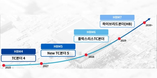
On July 15, Chairman Kwak Dong-shin issued a press release stating that the company would develop a hybrid bonder for HBM6 with a target launch at the end of 2027. He also added that memory makers would not use the expensive hybrid bonder for HBM5 production.
However, this diverges considerably from what I’ve learned from sources.
According to a source familiar with the matter, Samsung is aiming to apply hybrid bonding starting from HBM4E 16-high, while SK hynix is targeting HBM4E 20-high.
The source also indicated that narratives claiming hybrid bonding is difficult due to contamination are not accurate.
Given this, I think the CFO’s apparent shift in stance is essentially an attempt to change the market’s view that Hanmi is disadvantaged in hybrid bonding.
Even so, I recommend a Sell position on Hanmi Semiconductor.
I will cover Hanmi Semiconductor in more detail later in this piece.
One thing many people overlook about hybrid bonding is that the hybrid-bonding tool itself is relatively easy to build.
That’s why companies that wouldn’t dare enter the thermo-compression (TC) bonder market are targeting hybrid bonding as a new revenue stream.
In that sense, the hybrid-bonding tool itself is easy to make—especially for HBM applications.
The real bottleneck is chemical mechanical planarization (CMP) equipment.
What is CMP?
In hybrid bonding, the planarity, cleanliness, and uniformity of the bonding interfaces determine yield—in other words, the surface must not be uneven.
The process that creates this flat surface is the CMP process.
If, during simultaneous planarization of copper (Cu) and the dielectric (mainly SiOₓ, with some SiCN), you fail to hit nanometer-level specs for roughness, dishing/recess (Cu recess), and WIW (within-wafer) uniformity, both the oxide–oxide bond and the Cu–Cu electrical contact will break down.
So what exactly does CMP do?
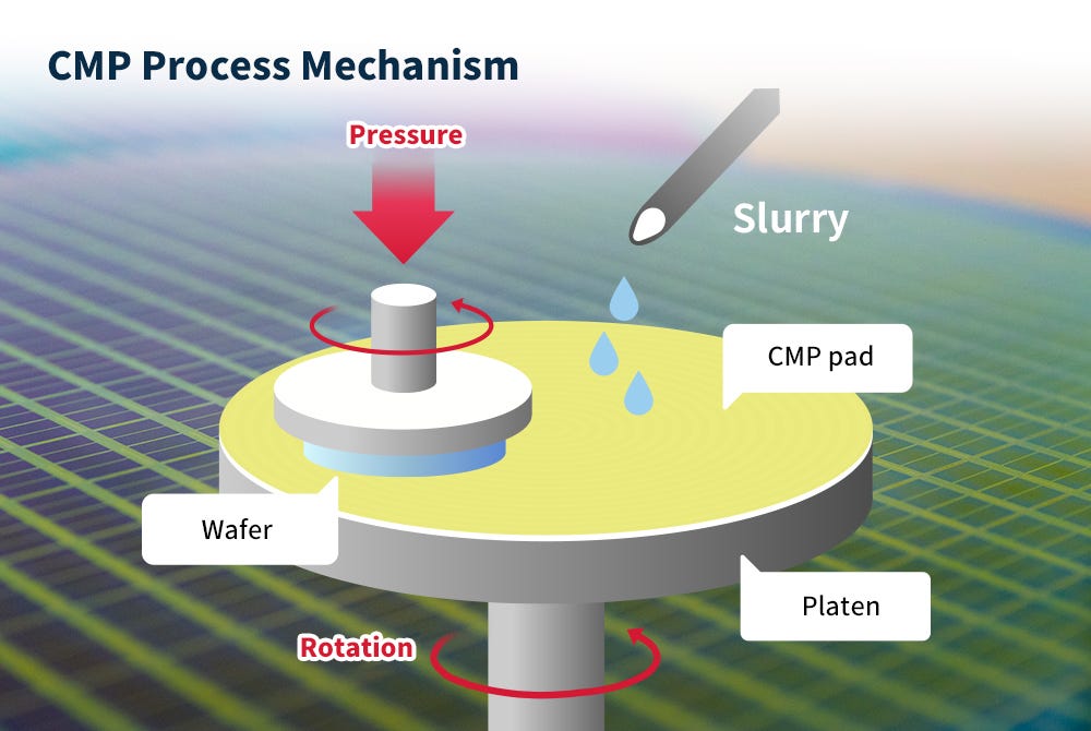
CMP (Chemical Mechanical Planarization) combines chemical reactions with mechanical polishing to produce an ultra-planar surface. In hybrid bonding, the goal is to bring the Cu pads and the surrounding SiOₓ (or SiCN) to the same height while reducing surface roughness to the atomic scale. Once this flatness is achieved, the oxides can bond at low temperature, and then Cu–Cu makes gap-free contact to form a low-resistance connection.
Originally, CMP wasn’t needed for TC bonding.
That’s because TC bonding uses bumps as an intermediary to join semiconductor chips, and the spaces between bumps are filled with a compliant molding material, so flatness requirements aren’t stringent.
Hybrid bonding is different. Because chips are directly joined without separate bumps, surface planarity basically dictates bonding yield.
The problem is that AMAT literally has a 100% monopoly on CMP equipment for hybrid bonding.
AMAT also holds a 60% share of the overall CMP market, and in hybrid-bonding CMP, AMAT is, quite literally, the god.
In April this year, Applied acquired a 9% stake in the Netherlands’ Besi, becoming its largest shareholder. The two companies had already been collaborating in hybrid bonding, and the equity investment made their relationship even tighter.
Even now, in the advanced packaging market for logic, the “Applied (CMP) + Besi (hybrid bonder)” alliance has tremendous influence.
Industry insiders unanimously say that if hybrid bonding technology is introduced into the HBM (high-bandwidth memory) industry, the pair is likewise highly likely to dominate the market.
Just as Japan’s Lasertec mask inspection tools are bundled alongside ASML’s EUV lithography systems, the two companies’ equipment could be supplied in tandem.
There are alternatives in the CMP equipment market—Japan’s Ebara and Korea’s KC Tech—but neither has any track record of supplying CMP for hybrid bonding.
In the paywalled section that follows, I will cover which vendors are currently preparing to enter the hybrid bonder market, their respective strategies, and who I see as the potential winners.


