
7 Key Investment Ideas: The Train Keeps Moving No Matter the Noise
Wrapping Up a Tough Week and Turning the Page


Hello, readers.
I’m back with the first planned series, an “Investment Idea Roundup.”
To explain the background a bit, one reader pointed out that I seemed to be too heavily focused on memory, so I decided to come up with a new series.
This past week… was a nightmare for Korean tech stocks.
As Kioxia’s earnings were crushed, most Korean memory names were not spared from declines.
As I was the first in the industry to point out, I see the fall in Kioxia’s results as stemming from a misjudgment by management: Kioxia signed an LTA with Apple before this supercycle, so even though the earnings themselves were not that bad, they fell short of the market’s overly elevated expectations.
I remain bullish on AI hardware and maintain a positive view on the memory shortage.
Accordingly, I added more Korean memory stocks during this pullback.
That said, I’m growing a bit more worried about Kioxia itself. Recently, the Taiwan supply chain has been buzzing with rumors that SanDisk will end its JV with Kioxia and outsource NAND production to Taiwanese foundries to increase supply.
Considering that Kioxia has been able to compete thanks to its partnership with SanDisk… this is quite concerning from my perspective.
In this series, I will present investment ideas that can capture both structural changes and asymmetric opportunities looking ahead to 2026.
ASML
Innolight (Hong Kong)
AIXTRON
Google
Korean memory stocks
NAND photoresist
Glass fiber (Nittobo)
1. ASML(ADR)
ASML CEO Christophe Fouquet said,
“There is no scenario in which 2026 revenue will be below 2025.”
Just three months ago, he was cautious, saying he “could not guarantee growth,” but has now shifted to a stance of clear optimism.
I want to say that this optimism from ASML’s CEO is not at all without basis.
Let me explain why I am bullish on ASML.
TSMC, additional capacity expansion

According to Morgan Stanley’s analysis, after Nvidia CEO Jensen Huang met CC Wei in Taiwan, he asked TSMC to increase Nvidia’s 3nm capacity, and TSMC responded by agreeing to increase its 3nm capacity by up to 20,000 wafers.
Originally, TSMC’s 3nm capacity for 2026 was projected at 140,000–150,000 wafers per month, but this is now expected to rise to 160,000–170,000 wafers per month.
What’s interesting is that this capacity increase does not directly translate into new EUV orders for ASML.
Local supply-chain interviews conclude that TSMC can handle this by driving the output and utilization of its existing EUV tools to extreme levels.
That said, here is what I want to emphasize:
“TSMC, which is unusually conservative in executing CAPEX, chose to expand capacity.”
This implies that the strength of AI demand is far higher than previously expected,
and in turn, this is directly linked to an acceleration of the transition to High-NA EUV at the A16 node and beyond.
In addition, the current approach of coping with more advanced nodes through multi-patterning on existing EUV tools is also expected to soon hit its limits, which allows us to foresee an expansion in High-NA EUV sales.
In other words, this round of capacity expansion should be interpreted not as “TSMC is placing incremental orders with ASML right now,” but rather as “an eventual explosion of EUV demand at the high-end nodes is unavoidable.”
The delay of 3D DRAM and the inevitability of EUV adoption

This is, in my view, the core pillar of the ASML bull thesis.
Within the memory industry, the prevailing view used to be that 3D DRAM would be adopted at the 1c node, or at the very least at 1d.
The goal was to stack 24–36 layers.
However, as 6F square has continued to evolve, it now appears that 3D DRAM will not be adopted until after 2033.
By that time, the layer count will need to be on the order of 90–100, whereas the 3D DRAM that each company has developed so far tops out at around 16 or 24 layers.
As a result, the current consensus is to first cover 3–4 generations with 4F square in the interim, and then move on to 3D DRAM afterward.
6F square and 4F square refer to the minimum cell area in DRAM. In a 6F square structure, a single cell is a rectangle of width 3F and height 2F (area = 6F square), whereas in 4F square it is a square of 2F by 2F (area = 4F square). By transitioning to 4F square, you can theoretically fit 30–50% more cells within the same chip die size. This is advantageous in terms of density, speed, and power, but it also creates the challenge of having to place the gate, channel, and capacitor on a much smaller cell area.
3D DRAM, on the other hand, inevitably “relieves” EUV demand within the DRAM industry.
The reason is that, just as in today’s NAND flash, it adopts a structure that stacks upward, which reduces the pressure for extreme node scaling and lowers EUV dependency per bit.
Instead, the center of gravity in equipment demand shifts sharply toward etch, deposition, CMP, plasma processes, and inspection/metrology.
However, because of the current technological hurdles, 3D DRAM has been pushed back to beyond 2033, and as the industry progresses in the order of 6F square → 4F square → 3D DRAM, EUV demand in the DRAM industry is expected to surge at least up through the 4F square phase.
I will go so far as to make what is probably the boldest call in the industry: I see a possibility that EUV demand from the three DRAM makers will surpass that of the three foundries (TSMC, Intel, and Samsung Foundry).
2. Innolight (HongKong)

A specialist in ultra-high-speed optical transceivers (Optical Transceiver) headquartered in Shenzhen, China, and currently one of the top-tier suppliers that delivers the largest volume to global hyperscalers (especially the U.S. Big 3).
Main products: 400G, 800G, 1.6T optical modules
Main customers: AWS, Meta, Microsoft, Google
Market position: More than 70% of revenue comes from North American CSPs
Unlike Chinese local module vendors, it makes “ultra-high-speed products for global CSPs.”
In other words, Innolight can be seen as a company whose revenue structurally grows together with the expansion of AI clusters.


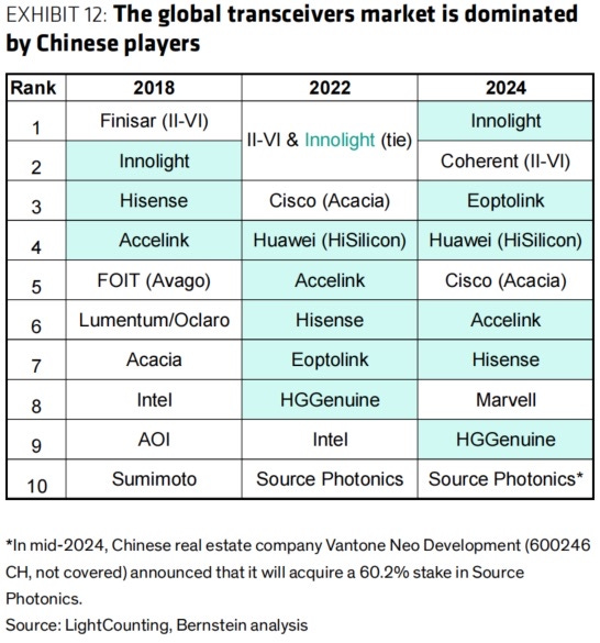
Originally, the U.S. government wanted to exclude Chinese companies from the optical module space.
However, the reality is completely different.
Because: if you exclude China, the build-out of AI infrastructure comes to a halt.
There are only a handful of companies in the world that can mass-produce 800G/1.6T optical modules quickly and cheaply
U.S./Israeli/Taiwanese vendors lag in production capacity (scale) and cost competitiveness
Players like Coherent and Lumentum have the technology but lack large-scale manufacturing capability
In the end, AWS, Meta, Microsoft, and Google all
cannot build out racks unless they buy high-speed optical modules from Chinese companies.
That’s why Innolight has become one of the few Chinese hardware companies that have been able to sidestep sanctions, and in return its dependence on U.S. CSPs has only increased.
I would argue that, over the medium to long term, this is not a “policy risk” but, on the contrary, a situation that becomes a moat.
Especially with Innolight set to list in Hong Kong next year, I’m very happy that I’ll finally be able to buy the king of Chinese optical modules.
I fully expect it to enjoy an H-share premium, and I want to classify Innolight as an irreplaceable Chinese company, like CATL.
3. AIXTRON (ETR: AIXA)

Power consumption of AI chips is increasing very rapidly. NVIDIA’s current Blackwell-generation GPU chips have already reached around 1.2 kW, and the power consumption of a GB200 rack-level server is about 120 kW.
The Rubin Ultra, scheduled for release in 2027, is expected to reach even three times the level of Blackwell. Rack-level server power consumption is projected to rise to around 600 kW.
By the time we reach the Feynman architecture, power is expected to increase by an additional 1.5x, exceeding 8x the current Blackwell level, and there is a high likelihood that rack-level server power consumption will reach around 1 MW (megawatt).
To solve this problem, NVIDIA has announced a new power system called “Kyber,” which adopts an 800V architecture. This dramatically increases the value of power semiconductors per system, and all the major power semiconductor companies are now competing to get into this supply chain.
At present, the value of the power semiconductors going into a single rack is about $12,000–$15,000. Taking the reference design and the increase in power demand into account, Barclays estimates that power semiconductor BoM content will increase more than sixfold by 2027, and then grow a further 50%+ by 2029, reaching roughly $140,000 per rack in today’s price terms.
However, the unfortunate reality is that there are simply too many players in power semiconductors today. Looking only at NVIDIA’s 800V partners, countless companies such as Navitas and Innoscience are already competing.
That is why I would recommend investing not in the miners working to dig up the gold, but in the company selling the pickaxes. In other words, the ASML of power semiconductors: AIXTRON.
According to Kerrisdale Capital, Aixtron’s MOCVD tools hold an overall market share of around 70%, and in several of the most attractive growth segments that figure exceeds 90%.
Notably, at a time when companies such as Infineon and TI are announcing the in-house production of 300mm GaN, AIXTRON is one of the very few vendors that offer 300mm GaN MOCVD tools.
Some worry about what happens if China localizes this equipment, but just as Kerrisdale’s supply-chain work suggests, my own interviews with industry contacts indicate that the technology gap between Chinese suppliers and AIXTRON remains substantial.
Kerrisdale Capital’s original report can be found here:
https://www.kerrisdalecap.com/investments/aixtron-aixa-gr/
4. Google

Apple’s strength lies in devices, Meta’s in advertising, Amazon’s in cloud, and Microsoft’s in Copilot and OpenAI — each has a clearly defined core competency.
By contrast, Google is the only company that simultaneously owns all of these pillars — literally the “Big Tech among Big Tech.”
And I believe that in the AI era, the company with the highest likelihood of building the most profitable AI business is also Google.
Let’s think through why.
First, Google has already secured an overwhelmingly dominant position in the market for search ad targeting.
In practice, there are very few platforms that can substitute for Google; the vast majority of global users, advertisers, and traffic sit on top of Google’s ecosystem.
Given this backdrop, Google has the highest probability of successfully integrating AI in a highly sophisticated way into its existing ad model.
The search, YouTube, Android, and Chrome ecosystems it has already built out are the largest distribution platforms in the world, and Google has the power to naturally layer new AI features and ad formats on top of them.
From the advertiser’s perspective, it’s actually very hard to refuse the new AI-based business tools Google offers.
Because, ultimately, “if you want your product to sell inside Google’s ecosystem, you have no choice but to follow Google’s algorithms.”
In other words, through a combination of its massive user base + advertiser dependence + proprietary AI infrastructure (TPU) + distribution platforms, Google is positioned to become the player with the highest margins and the strongest operating leverage in the AI era.
I also think many people are underestimating YouTube as a platform.
The more AI advances, the more AI-based creator tools will shine (subtitles, auto-cut editing, multilingual translation).
And as AI drives the cost of production in creative work toward zero, YouTube upload volume will increase in a near-linear explosion.
This, in turn, will expand ad inventory, make ads more sophisticated, and structurally grow revenue.
Lastly, there is Google Cloud.
A lot of people still treat Azure and AWS as the only truly meaningful players in the market, but I would argue that Google Cloud has a tremendous opportunity ahead.
Azure does not have its own large language model and is overly dependent on OpenAI, while OpenAI is trying to break away from Microsoft.
Meanwhile, AWS’s Trainium and Inferentia performance is frankly very poor.
Google Cloud, with Vertex AI + TPU + Gemini API, owns a vertically integrated SaaS/infra stack —
which effectively makes Google Cloud the only hyperscaler that is independent of the GPU stack.
Why do you think so many large customers — xAI, Anthropic, Meta, and others — want to keep using Google Cloud?
To sum it up in one sentence, in the AI era, the only company that combines the highest potential, the lowest cost structure, and the broadest user base distribution is Google.
The following section is behind a paywall.
Beyond the paywall, you’ll find:
• My view on the current memory supercycle
• My overall outlook on Korean memory stocks
• Some interesting insights on photoresist used in memory that I picked up from recent supply-chain checks
• Updates related to fiberglass
